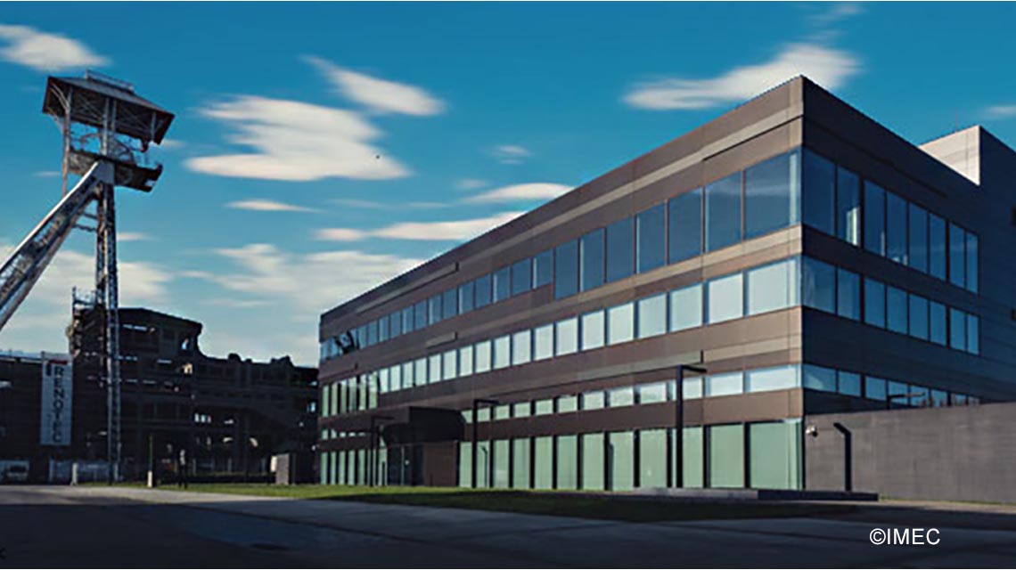
IMEC - ThinFilm PV Lab
Our perovskite assembly line allows to process full modules up to 35x35cm². A slot die coater can deposit solution-based materials while a vacuum thermal evaporation, with 4 sources, and sputtering system, with RF and DC targets, makes a combination of oxide and metallic coatings accessible for both passivation and electrode layers. We developed soft sputtering processes for metal oxides atop perovskite stack without causing damage to the underneath fragile layer stack. In particular, we do not need atomic layer protection layer, which is typically used in the literature, to prevent bombarding induced damage from ITO sputtering for semi-transparent perovskite cells and modules. In addition, a versatile 3-wavelength picosecond laser system is available for the creation of very narrow interconnections between adjacent cells in the modules. Dispenser and curing stations are available to complete the module packaging. All of these tools are integrated in or connected to controlled atmosphere gloveboxes. A double membrane laminator and screen-printers for patterned metal contacts are also availabe in ambient atmosphere. This enables to create opaque or semi-transparent modules, either rigid or flexible.
Several material and device characterization techniques are available, ranging from scanning electron microscope, Dektak profilometer and 3D confocal microscope, time-resolved photoluminescence, UV-Vis absorbance-reflection measurements, Hall effect, sheet resistance, electroluminescence imaging and high-resolution spectral response to climate chambers for damp heat, thermal cycling and UV testing.
Several class A solar simulators, in ambient as well as in inert atmosphere, are operational for small area devices up to 10x10cm2 modules. Characterization of the large area modules can be done with a large-area LED-light-based solar simulator which can provide A+A+A+ light quality over 1x1.6m2 area and also integrated back lighting for bifacial modules. Electroluminescence measurement of full-size modules with a resolution of <150 um is also possible in the same setup.

This project has received funding from the European Union’s Horizon 2020 research and innovation programme under grant agreement N°101006715
